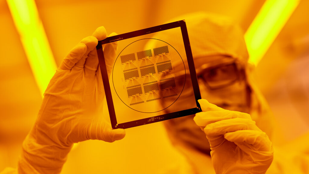
SRI’s cleanroom offers clients the ability to develop new devices, build prototypes, work with experts, and run small-scale manufacturing.
Semiconductors play a crucial role in our modern, technology-fueled world. They’re at the heart of our cell phones, computers, and other electronics receiving, processing, and storing information. The process of manufacturing semiconductors must be precisely controlled — contamination by even a few unexpected molecules can change a semiconductor’s properties and alter a chip’s performance.
“These systems are very sensitive to chemical and physical impurities,” said Christopher Chua, senior manager of the micro-technology group and a principal research scientist at SRI. “The features we are trying to make are very small — if one speck of dust lands on an unintended area, the whole circuit could stop working. From water to air, everything must be controlled.”
SRI maintains a set of cleanroom facilities in one location for semiconductor microfabrication that enable researchers to develop new semiconductor devices and production processes, build prototypes, and transition new technologies to commercial manufacturing. These facilities are used by SRI researchers and are also available to clients for product development, as well as small-scale manufacturing. Example capabilities include atomic layer deposition, chlorine-based ICP, ultra-wide bandgap epitaxial growth, doped amorphous silicon PECVD, low-pressure chemical vapor deposition, excimer laser shallow dopant activation, and physical deposition of films such as ITO and superconducting materials.
An advanced space for multiple chip processes
“Most cleanroom services only offer singular microfabrication steps, such as thin film deposition or wafer thinning,” Chua said. “Here in Palo Alto, we offer custom process development spanning across an entire spectrum of microfabrication processes, and we have a wide variety of know-how and equipment in one location. We work with clients to understand what they need and then develop new, specialized processes in collaboration, facilitating both prototype development and lab-to-fab transitions.”
Most semiconductors are created through multiple processes, and each step affects what comes next. If a problem arises, it’s not sufficient to adjust a single micro-fabrication step. SRI researchers have a holistic view of device physics, materials, and capabilities to optimize across multiple process steps.
“In Palo Alto, we offer custom process development spanning across an entire spectrum of microfabrication processes, and we have a wide variety of equipment in one location. ” — Christopher Chua
“We have in-house capabilities to efficiently make process and materials adjustments when developing semiconductor devices and fabrication processes,” Chua said. “When we’re trying things that have never been done, we also frequently build custom equipment.”
Leading provider of thin-film transistors and MicroLEDs
Prototyping thin-film transistor devices, in both amorphous- and poly-silicon, is one of the core capabilities of SRI’s cleanroom facilities. This technology is used in applications such as X-ray imager and laptop display backplanes, and flexible electronics. SRI’s facility is one of only a few places in North America that can prototype these types of devices.
MicroLED is an emerging technology that uses millions of tiny individual LEDs (each about the size of a red blood cell) to create display pixels. The technology offers significant improvements over current displays, but there are still unsolved technical problems, such as how to repair defective pixels within a sea of micro-LEDs. Today, our collaborators are using SRI’s cleanroom to address some of the challenges in manufacturing these displays.
In addition, the facility is used for developing semiconductor packaging technology, such as glass interposers, tiny chiplet pick-and-place, high density interconnect, laser diodes, avalanche photodetectors, large area electronics, and CMOS imagers.
To learn more about SRI’s cleanroom capabilities contact us today.